Saltar al contenido principal Saltar al pie de página
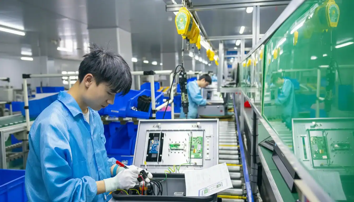
El diseño de una placa de circuito impreso de cargador de coche a medida suele ser el único punto de fallo que detiene el lanzamiento de un producto, lo que provoca costosos retrasos en la certificación y la pérdida de cuota de mercado. Muchos equipos de hardware intentan integrar funciones avanzadas como la carga del vehículo al hogar (V2H) y la carga solar en placas genéricas, pero se enfrentan a problemas insalvables con la gestión térmica, la comunicación entre componentes y el cumplimiento de la normativa. Este enfoque ad hoc crea un producto que no es fiable sobre el terreno ni certificable para el mercado.
Este informe técnico no se centra en las discusiones superficiales, sino en las decisiones críticas de I+D necesarias para el éxito de la construcción. Analizaremos los retos de ingeniería específicos, desde la integración de chips V2H bidireccionales en la placa base hasta los aspectos prácticos del uso de pinzas de TC inalámbricas para equilibrar la carga dinámica. También abordaremos las opciones a nivel de componentes, como la especificación de relés de nivel 1 para automoción, y esbozaremos un flujo de trabajo de prototipado rápido para obtener una muestra funcional fabricada en días, no en meses.
Preparado para Bi-Direccional: ¿Podemos añadir chips V2H a la placa base?
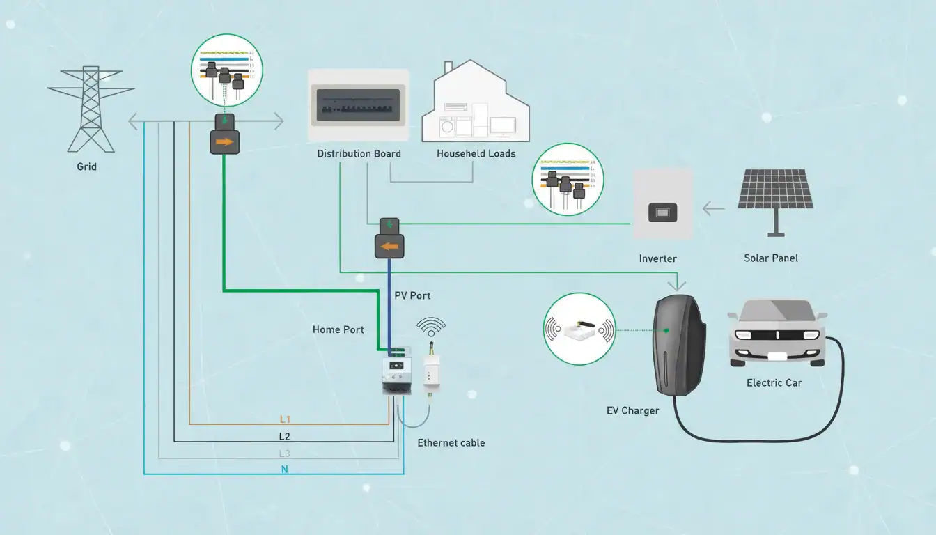
Actualmente, la funcionalidad de vehículo a hogar (V2H) se consigue mediante una arquitectura modular de componentes separados, no con un único chip integrado en la placa base del cargador.
Estándares actuales de hardware y protocolos
Los sistemas V2H actuales se basan en una arquitectura de hardware distribuida para gestionar el flujo bidireccional de energía. Las implementaciones utilizan inversores y convertidores dedicados y separados para gestionar la exigente tarea de convertir la corriente continua de la batería del vehículo en corriente alterna sincronizada con la red para una vivienda. Esta gestión de la energía se coordina mediante protocolos de comunicación establecidos como CHAdeMO y SunSpec, que garantizan una transferencia de energía segura y fiable. Este enfoque modular es el estándar comercial predominante porque aísla eficazmente el proceso de conversión de alta potencia de la lógica de control principal, garantizando la estabilidad y seguridad del sistema.
| Componente | Arquitectura modular V2H actual | Hipotética solución de chip integrado |
|---|---|---|
| Conversión de potencia | Módulos inversores y convertidores externos dedicados. | Circuitos de conversión de alta potencia en chip. |
| Lógica de control | Gestionado mediante protocolos como CHAdeMO y SunSpec. | Sincronización de red y lógica de control integradas. |
| Gestión térmica | El calor se distribuye a través de múltiples componentes físicos. | Desafío de disipación de calor altamente concentrado. |
| Situación del mercado | Disponibles en el mercado y probados sobre el terreno. | Actualmente en fase de I+D; no es comercialmente viable. |
Retos técnicos de la integración directa
Integrar toda la funcionalidad V2H en un único chip de placa base introduce importantes barreras técnicas. Un solo chip tendría que gestionar tanto la conversión de alta potencia como la compleja lógica de control para la sincronización de la red, tareas que generan un calor considerable. La gestión térmica eficaz se convierte en un problema de ingeniería primordial; disipar el calor de un chip compacto e integrado sin comprometer el rendimiento o la vida útil es extremadamente difícil. Estos retos combinados de potencia, control y calor son la razón por la que la industria sigue confiando en componentes separados y especializados para garantizar la fiabilidad y seguridad operativas.
El futuro se centra en la miniaturización
A medida que se generaliza la carga bidireccional, el objetivo estratégico del sector a largo plazo es la miniaturización. La I+D se centra en reducir el tamaño físico y el coste global del sistema de la tecnología V2H. Este progreso depende en gran medida de los avances en el diseño de semiconductores, que podrían dar lugar a soluciones más integradas y compactas. Esta innovación es esencial para que los cargadores bidireccionales sean más asequibles, accesibles y fáciles de instalar por los electricistas en entornos residenciales y comerciales.
Equilibrio dinámico de la carga (DLB): ¿Es posible la integración de pinzas de TC inalámbricas?
En 2026, la integración de pinzas CT inalámbricas para el equilibrio dinámico de la carga será una solución madura y estándar, impulsada por sus enormes ventajas en coste de instalación y escalabilidad frente a los sistemas tradicionales cableados.
La integración inalámbrica será una práctica habitual en 2026
Sí, la integración de pinzas de TC inalámbricas para el equilibrado dinámico de la carga (DLB) no sólo es posible, sino que ya es una tecnología madura y ampliamente adoptada. En KelyLands, confirmamos que este enfoque es estándar tanto para instalaciones nuevas como de modernización. Elimina por completo la necesidad de complejos y costosos cableados desde el cargador hasta el cuadro eléctrico principal. El mercado se ha decantado decididamente por la tecnología inalámbrica para facilitar un rápido despliegue de la infraestructura.
- El mercado se ha decantado decididamente por las soluciones inalámbricas para facilitar la rápida ampliación de la infraestructura.
- Nuestros cargadores para vehículos eléctricos están diseñados para ser compatibles con los principales sistemas inalámbricos de control de la energía.
Ventajas de instalación y escalabilidad
La principal ventaja de un sistema DLB inalámbrico es la reducción significativa de la complejidad y el coste de la instalación. Evita la necesidad de costosas obras eléctricas, como la instalación de nuevos conductos o la excavación de zanjas para cables. Esto agiliza el despliegue y lo hace mucho más escalable, especialmente en grandes propiedades comerciales, complejos de apartamentos o edificios ya existentes en los que no es factible realizar obras molestas.
- Las pinzas inalámbricas para TC permiten realizar instalaciones de reequipamiento sin necesidad de grandes reformas eléctricas.
- Los clientes pueden desplegar y ampliar sus redes de recarga de forma más eficiente gracias a los menores costes iniciales de mano de obra y material.
Protocolos de comunicación clave: LoRa, WiFi y RF
Nuestro equipo de ingenieros integra varios protocolos de comunicación inalámbrica para satisfacer los distintos requisitos de los emplazamientos. LoRa es excelente para la cobertura a larga distancia en grandes zonas de aparcamiento, mientras que WiFi y RF son fiables y rentables para las típicas instalaciones residenciales y comerciales. La elección del protocolo adecuado depende totalmente del entorno de instalación y de las necesidades de rendimiento.
| Protocolo | Caso de uso óptimo | Características principales |
|---|---|---|
| LoRa (largo alcance) | Grandes propiedades comerciales, amplios aparcamientos. | Excelente cobertura a larga distancia (hasta ~300 m); ideal para superar barreras físicas. |
| WiFi | Instalaciones residenciales y comerciales estándar con infraestructura de red existente. | Aprovecha las redes existentes; integración perfecta con los sistemas inteligentes de gestión de la energía. |
| RF (radiofrecuencia) | Conexiones fiables punto a punto en entornos de edificios típicos. | Comunicación sencilla y robusta; menos propensa a la congestión de la red que WiFi. |
Rendimiento: Soluciones cableadas frente a inalámbricas
Aunque la conexión inalámbrica es la opción dominante por su flexibilidad, KelyLands también admite pinzas de TC cableadas para casos de uso específicos. Una conexión por cable ofrece una fiabilidad absoluta de latencia cero y es inmune a las interferencias de red. Esto la convierte en la opción preferida para aplicaciones industriales de misión crítica o emplazamientos con interferencias de radiofrecuencia extremas en los que el rendimiento garantizado tiene más peso que la comodidad de instalación.
- Las soluciones inalámbricas son ideales para la mayoría de los usos comerciales y residenciales en los que la flexibilidad es clave.
- Las conexiones por cable ofrecen la máxima resistencia fuera de línea para los sitios que requieren ajustes de carga garantizados e instantáneos.
Su marca en los cargadores inteligentes certificados para vehículos eléctricos

El uso de relés de automoción es innegociable para fabricar cargadores de vehículos eléctricos duraderos, ya que están diseñados para soportar cargas de alta intensidad y condiciones ambientales extremas que los componentes comerciales estándar no pueden soportar con fiabilidad.
La decisión de utilizar relés de nivel 1 para automoción afecta directamente a la seguridad, fiabilidad y viabilidad comercial a largo plazo de un cargador de VE. Aunque los componentes de calidad comercial pueden reducir los costes de producción iniciales, introducen importantes riesgos de fallo cuando se someten a las altas corrientes sostenidas y a los duros entornos operativos habituales en la infraestructura de carga. Los relés de automoción están diseñados específicamente para mitigar estos riesgos, lo que los convierte en la opción de ingeniería correcta para construir un producto robusto.
Rendimiento y fiabilidad a altas temperaturas
Los relés para automoción están diseñados para funcionar de forma fiable en un amplio rango de temperaturas, normalmente de -40 °C a +125 °C. Esta estabilidad operativa es fundamental para los cargadores de vehículos eléctricos que deben funcionar en diversos climas del mundo sin degradar su rendimiento. Tanto si se instala en un garaje escandinavo helado como en un aparcamiento soleado de Oriente Medio, la función de conmutación principal del componente se mantiene constante. Esto se combina con una gran longevidad mecánica, con valores que a menudo superan el millón de ciclos, lo que reduce drásticamente el riesgo de fallo del componente a lo largo de la vida útil del cargador.
| Característica | Relé comercial | Relé para automoción (Nivel 1) |
|---|---|---|
| Temperatura de funcionamiento | Estrecha (por ejemplo, de 0°C a 70°C) | Ancho (-40°C a +125°C) |
| Longevidad mecánica | ~100.000 - 300.000 ciclos | 1.000.000+ ciclos |
| Sellado medioambiental | A menudo sin sellar o parcialmente sellado | Diseño totalmente sellado (a prueba de polvo y humedad) |
| Resistencia a las vibraciones | Estándar | Alta; diseñada para entornos de vehículos |
Capacidad de conmutación de alta corriente
Estos relés están diseñados para gestionar las importantes cargas eléctricas de la carga de vehículos eléctricos. Hay disponibles modelos capaces de conmutar hasta 130 A, que gestionan con seguridad el amperaje necesario para las sesiones de carga rápida en unidades de 7 kW, 11 kW y 22 kW. Esta capacidad es esencial para un suministro de energía seguro y eficiente. También incorporan una gestión térmica mejorada para evitar el sobrecalentamiento durante un uso continuado de varias horas, una situación habitual que puede provocar el fallo de componentes menores.
Sellado ambiental y durabilidad
Un diseño totalmente sellado protege los mecanismos internos del relé del polvo, la humedad y otros contaminantes ambientales. No se trata de un lujo, sino de un requisito para los equipos que se instalarán en el exterior y estarán expuestos a los elementos. Esta robusta construcción garantiza la durabilidad a largo plazo, protegiendo contra la entrada y soportando los impactos físicos y las vibraciones que pueden producirse durante el transporte, la instalación y el uso diario. Una parte esencial de nuestra filosofía de diseño consiste en suministrar relés que cumplan las estrictas normas de conformidad para entornos exigentes.
Prototipado rápido: ¿Podemos imprimir en 3D una muestra funcional en 7 días?
Un prototipo de cargador de vehículo eléctrico funcional impreso en 3D en siete días no sólo es posible, sino que forma parte de nuestro proceso de desarrollo de OEM, gracias a la fabricación digital moderna.
De semanas a días: Velocidades actuales de creación de prototipos
La norma industrial para la creación rápida de prototipos ha cambiado radicalmente. Los ciclos de fabricación que antes duraban semanas ahora se reducen a sólo 24 o 72 horas para muchos componentes. KelyLands aprovecha estos avances para hacer que un plazo de 7 días para una muestra funcional sea un objetivo práctico para la mayoría de los proyectos de OEM.
- La fabricación aditiva avanzada comprime los plazos tradicionales de producción de placas de circuito impreso y carcasas.
- Para diseños específicos, podemos fabricar prototipos funcionales en cuestión de horas, lo que permite una validación inmediata del diseño.
- Esta velocidad reduce los costes de desarrollo y acelera todo el ciclo de comercialización del producto.
Tecnologías básicas para una entrega rápida
Nuestro proceso de creación de prototipos utiliza tecnologías clave de fabricación digital que obvian la necesidad de utillaje tradicional en las primeras fases. Esto permite la creación directa e inmediata de piezas complejas a partir de diseños digitales.
- La impresión 3D de precisión crea carcasas físicas multicapa y complejas directamente a partir de archivos CAD.
- Los sistemas de imagen directa y el procesamiento por láser permiten fabricar rápidamente placas de circuito impreso funcionalmente complejas.
- Estas herramientas ofrecen la flexibilidad necesaria para personalizar las geometrías de las placas y realizar cambios rápidos e iterativos en el diseño.
Viabilidad y proceso de 7 días de KelyLands
Un prototipo de 7 días es factible y se ajusta a nuestro plazo de entrega de muestras estándar de 7 a 15 días. El proceso comienza con una revisión del diseño para confirmar que la complejidad de los componentes y las necesidades de material se ajustan a los plazos de producción rápida.
- El objetivo de 7 días suele abarcar una muestra funcional inicial con piezas impresas en 3D y una placa de circuito impreso verificada.
- El plazo final depende de la complejidad del proyecto, la disponibilidad de material y el alcance de las pruebas funcionales necesarias.
- Esta fase de prototipado rápido es una parte estándar de nuestro servicio OEM/ODM antes de comprometernos con la fabricación de herramientas para la producción en serie.
Conclusión
La creación de un cargador para vehículos eléctricos listo para el mercado empieza en la placa base. La integración de funciones como la preparación V2H y el equilibrio de carga dinámico inalámbrico directamente en la placa de circuito impreso crea un producto potente y eficiente. La selección de componentes de automoción para el diseño garantiza la fiabilidad y seguridad a largo plazo para el usuario final.
Si está desarrollando un cargador EV personalizado, nuestro equipo de ingeniería puede ayudarle a validar sus requisitos de hardware. Póngase en contacto con nosotros para hablar de las especificaciones de su proyecto y explorar nuestras soluciones OEM.
Preguntas frecuentes
¿Pueden diseñar una placa de circuito impreso personalizada para mi cargador?
Por supuesto. Estamos especializados en el diseño y desarrollo de placas de circuito impreso personalizadas para cargadores de vehículos eléctricos. Nuestro proceso implica un enfoque de colaboración en el que trabajamos con su equipo para definir los requisitos específicos, incluido el factor de forma, las especificaciones de potencia, los protocolos de comunicación y las características exclusivas. Nos encargamos de todo el ciclo de vida, desde el diseño esquemático y la selección de componentes hasta el diseño, la creación de prototipos y las pruebas, para garantizar que la placa final cumpla sus objetivos de rendimiento, coste y certificación.
¿Son compatibles con el hardware V2H (Vehicle to Home)?
Sí, admitimos la integración de hardware de vehículo a hogar (V2H). Nuestra arquitectura de hardware actual para la carga bidireccional utiliza un enfoque modular con inversores y convertidores dedicados para gestionar eficazmente el flujo de energía y la sincronización con la red. Este diseño garantiza un rendimiento sólido y el cumplimiento de protocolos de comunicación establecidos como CHAdeMO y SunSpec. A medida que evoluciona la tecnología, nos centramos activamente en la I+D de soluciones más compactas e integradas que utilicen semiconductores avanzados.
¿Qué marcas de relés y condensadores utiliza?
Para componentes críticos como relés y condensadores, nos abastecemos exclusivamente de fabricantes de primer nivel líderes del sector para garantizar la máxima fiabilidad y seguridad. Nuestros proveedores preferidos de relés de alta potencia incluyen marcas como TE Connectivity, Omron y Panasonic. En cuanto a los condensadores, normalmente especificamos componentes de larga vida útil y resistentes a altas temperaturas de fabricantes como TDK, Murata, Nichicon y KEMET. La selección de componentes se adapta siempre a los requisitos específicos de tensión, corriente y entorno de la aplicación.
¿Podemos añadir un módulo 4G/LTE a la placa?
Sí, podemos integrar un módulo 4G/LTE en el diseño de la placa de circuito impreso de su cargador. Normalmente utilizamos módulos M.2 o mini-PCIe precertificados de proveedores líderes como Sierra Wireless, Telit o u-blox para acelerar el desarrollo y simplificar las aprobaciones de los operadores. El proceso de integración incluye el diseño de las interfaces de alta velocidad necesarias, la colocación adecuada de la antena para una integridad óptima de la señal y la gestión del consumo de energía del módulo.